


 Is India’s Electronics Game-Changer")
India’s electronics growth story will not be written by assembly alone. Embedding Design for Manufacturing into every stage of product creation is the step that can transform ambition into global competitiveness—and make India a genuine leader in electronics.
India’s push toward self-reliance in electronics is being tested across high-stakes sectors—defence, railways, energy, aerospace, and industrial systems—all of which demand hardware that is rugged, reliable, and scalable. The old model of import dependence and assembly is giving way to something far more ambitious: electronic design for manufacturing (DFM). No longer a peripheral practice, DFM has become the foundation for producing hardware that meets global standards while withstanding real-world operating challenges, making it indispensable to India’s rise as a serious electronics contender.
The Indian electronics ecosystem: Context and imperatives
Defence, aerospace, railways, oil and gas, and renewable energy are all moving rapidly towards digitisation, creating a surge in demand for hardware that can withstand harsh conditions while delivering consistent performance. Meeting this demand requires more than incremental upgrades—it calls for a design philosophy that anticipates scale, reliability, and manufacturability from the outset.
For example, Indian Railways is undertaking the large-scale deployment of connected systems to enhance both operational efficiency and safety across its vast network. At the same time, Industrial IoT is transforming key sectors such as oil and gas, manufacturing, and energy, necessitating the use of robust gateways and intelligent edge devices to ensure reliable data processing and connectivity. Meanwhile, the consumer electronics market continues its rapid expansion, fuelling demand for innovative, high-quality products that meet evolving user expectations.
This evolution is underpinned by a national push for ‘Made in India’ electronics, not just as an assembly hub, but as a design and manufacturing powerhouse. Geopolitical shifts and supply chain disruptions have opened opportunities for India to emerge as an alternative to China. However, this also exposes vulnerabilities, especially in component sourcing, R&D infrastructure, and manufacturing maturity.
DFM: Principles and technical foundations
DFM is an engineering approach focused on creating electronic products that are optimised for manufacturing, assembly, testing, and long-term performance. By incorporating DFM principles early in the design process, engineers ensure that products are easy to manufacture at scale, maintain consistent quality, remain cost-effective, comply with relevant industry standards, and perform reliably in real-world conditions.
DFM is central to ensuring that the product moves seamlessly from concept to production. A design should not only be functional at prototype stage but also robust enough to be fabricated, assembled, and tested repeatedly and reliably.
| Principle | Description |
| Simplicity and standardisation | Minimise complexity, use standard components, and avoid proprietary or hard-to-source parts |
| Manufacturing process alignment | Design PCBs and assemblies compatible with local manufacturing capabilities |
| Testability | Integrate test points, diagnostic interfaces, and validation hooks from the outset |
| Thermal and EMI/EMC design | Optimise layouts for heat dissipation and electromagnetic compliance |
| Documentation and traceability | Maintain detailed schematics, BOMs, and revision histories |
| Compliance planning | Embed regulatory and certification requirements into the design phase |
| Lifecycle considerations | Plan for upgrades, maintenance, and end-of-life management |
The benefits of DFM are significant across the product lifecycle. By minimising production defects and the need for rework, DFM helps lower overall manufacturing costs. It also facilitates improved automation and scalability, enabling more efficient production processes. Additionally, DFM contributes to enhanced product quality and higher customer satisfaction, while accelerating time-to-market for new products.
India-specific DFM challenges
India remains heavily dependent on imported components—especially semiconductors, sensors, and advanced displays. This exposes the supply chain to cost fluctuations and delays.
Manufacturing infrastructure limitations include:
PCB fabrication: Advanced PCBs (e.g., > 6 layers, fine traces) are challenging to source locally, especially for low-volume runs.
Enclosure fabrication: Quality, low-volume enclosure manufacturing is limited, affecting start-ups and SMEs.
Testing labs: Access to certified, third-party testing facilities is scarce, causing delays in validation and compliance.
Skills and ecosystem gaps include:
Design expertise: Many engineers lack experience in DFM, compliance, and system reliability.
Academia-industry disconnect: Curricula often lag behind industry needs, especially in applied design and compliance engineering.
Prototyping ecosystem: The ecosystem for rapid prototyping and validation is still maturing, with long lead times and regulatory hurdles. India has proven itself a global software powerhouse. However, many software engineers entering embedded domains are not trained in systematic hardware–software co-design. Start-ups and SMEs, while nimble, often lack the luxury of time or structured mentorship. As a result, firmware engineers are often pushed into projects with a “code-first” mindset—writing code without proper architecture, documentation, or planning. This approach can quickly lead to unscalable, untestable, and difficult-to-debug codebases.
Go-to-market pressures: Hidden risks for start-ups and SMEs
Start-ups and SMEs racing to launch products often take shortcuts—replicating reference designs without adaptation, skipping critical reliability tests, or using educational platforms like Arduino or Raspberry Pi in production. While fast, these choices lead to immature, failure-prone products, damaging brand credibility and eroding market trust.
A common and costly mistake is selecting the wrong development toolchain early on. Developers may later realise their tools carry restrictive licences, or lack support for production or certification—forcing last-minute rewrites that delay launches and inflate costs. In high-stakes domains like automotive, this can mean redoing entire codebases. Choosing a toolchain should go beyond features—it must account for licensing, update cycles, and long-term sustainability.
DFM best practices: Technical methodology
DFM requires a structured approach, starting with thorough requirement capture and extending through to compliance and certification. The first step involves requirements engineering, where teams define the product’s functional features, including the required interfaces and communication protocols. Environmental constraints such as temperature, humidity, vibration, altitude, and ingress protection (IP ratings) must be considered. Safety and regulatory compliance (e.g., IEC, UL, EMI/EMC, RoHS, and ATEX/IECEx for hazardous environments) also need to be clearly understood. Lifecycle planning is critical to account for component longevity, upgrade paths, and overall maintainability.
The system architecture phase translates requirements into a functional design, using block diagrams to break down subsystems such as compute, power, communications, sensors, and interfaces. Flowcharts and state machines help define software behaviour, including event handling and fault management. Security must be integral from the start, incorporating secure boot, key storage, encrypted communications, and robust authentication protocols.
In India’s electronics design landscape, two priorities stand out—delivering real customer value and ensuring design sustainability. Many teams lose time in avoidable rework due to poor upfront planning. Thoughtful design extends beyond function; it lays the groundwork for scalable and efficient product development. The key is to design with mass manufacturing in mind from the start—incorporating test hooks, debugging interfaces, and field diagnostics early on to avoid delays and cost overruns later.
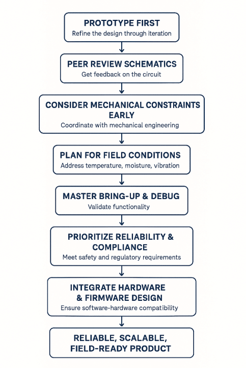
Prototyping and validation are essential to reduce risks early in the development cycle. Prototypes using evaluation boards or development kits help validate core concepts before investing in custom hardware. Peer reviews of schematics and PCB layouts help identify design flaws and improve quality. Mechanical fit and clearance issues are addressed through 3D modelling using electronic design automation (EDA) tools, which also aid in thermal path analysis.
During the PCB and mechanical design stage, layouts must support DFM principles by optimising trace routing, thermal management, and minimising EMI/EMC issues. Component placement should facilitate automated soldering, inspection, and possible rework. Mechanical design must align with enclosure constraints, mounting provisions, and withstand environmental stressors.
Testability and production readiness are enhanced by embedding test points and interfaces for in-circuit testing, firmware flashing, and diagnostic access. It is important to design for remote debugging, crash logging, and field upgrades to simplify post-deployment support. Meticulous documentation—including design files, test procedures, and traceability records—is crucial for efficient manufacturing and long-term support.
Finally, compliance and certification processes should begin early, with pre-compliance testing in specialised labs to catch EMI/EMC and safety issues. Regulatory submissions demand thorough documentation and test evidence. Each technical requirement should be linked to a corresponding test case, ensuring traceable and verifiable compliance throughout the product lifecycle.
Embedded system and IoT gateway design: A practical example
Designing a reliable embedded system and IoT gateway begins with a clear definition of the system scope and mission—what the device is intended to do and the environment it will operate in. Choosing the right microcontroller and hardware components is critical, with emphasis on reliability, power efficiency, and built-in security features. The firmware architecture should be modular and maintainable, with support for over-the-air (OTA) updates to enable future enhancements and bug fixes. Hardware–software co-design plays a vital role, requiring close collaboration between hardware and firmware teams to achieve seamless integration, optimal performance, and efficient development cycles.
The IoT gateway serves as the bridge between embedded devices and cloud or enterprise systems. On the hardware side, it must have sufficient processing power and memory to handle data aggregation, edge analytics, and protocol translation in real time. Multi-protocol connectivity is a must—supporting Ethernet, Wi-Fi, LTE, RS485, CAN, BLE, Modbus, OPC UA, and more—to ensure compatibility with diverse devices and networks. Industrial use cases demand ruggedisation against environmental factors like temperature extremes, humidity, vibration, and dust ingress, with protection ratings such as IP54, IP65, or IP68. Robust power management options, including battery, mains, or solar sources with backup systems and low-power modes, further enhance reliability in the field.
From the software and security perspective, the gateway may run a real-time operating system (RTOS) or embedded Linux, depending on the complexity and latency requirements of the application. Edge computing capabilities allow for local data processing, filtering, and analytics, reducing dependency on cloud bandwidth. Security is foundational—requiring encrypted communication, secure boot, hardware-based root of trust, and role-based access control to protect against cyber threats.
For integration and interoperability, the gateway must support protocol translation, enabling seamless communication between legacy systems and modern IoT devices. A modular architecture based on APIs and microservices ensures scalability and simplifies integration with other systems. Remote management features such as firmware updates, remote configuration, and diagnostics allow for efficient deployment and maintenance.
Finally, attention to compliance and reliability ensures long-term operability and trust. This includes adhering to relevant safety and EMC standards, such as IEC 61508 and ISO 26262, along with thorough reliability testing, including thermal cycling, vibration, and environmental stress simulations. Choosing components from reputable suppliers with guaranteed availability and documented end-of-life (EOL) timelines strengthens the foundation for a sustainable and certifiable IoT solution.
DFM in practice: Workflow and best practices
A robust DFM workflow is crucial to transforming a concept into a reliable, scalable, and cost-effective electronic product. The end-to-end process begins with clear requirements capture and thorough documentation to align design intent with functional goals. System architecture and block diagrams are then developed to map out major components and interfaces. Prototyping and proof-of-concept validation follow, serving to de-risk core functionality early in the cycle.
Next, schematic capture and peer reviews ensure design integrity before proceeding to PCB layout, which incorporates DFM checks to catch manufacturability issues early. This is followed by mechanical and thermal validation to confirm fit, heat dissipation, and durability under operating conditions.
The integration of test points, along with detailed production planning, lays the groundwork for streamlined assembly and debugging. Compliance and pre-certification testing ensure that regulatory requirements are addressed upfront, while pilot production enables iterative refinement based on real-world feedback. At every stage, detailed documentation and design traceability support lifecycle management and future upgrades.
Key technical best practices further strengthen the DFM process. These include designing for simplicity and manufacturability, collaborating early with manufacturing and supply chain partners, and leveraging industry-standard EDA tools equipped with built-in DFM rule checks. Planning for automation and reducing manual intervention not only speeds up production but also enhances consistency. Comprehensive documentation is vital to support traceability, version control, and long-term support. Most importantly, testing must go beyond lab conditions to include real-world scenarios, ensuring that the product performs reliably in its intended environment.
DFM as the foundation for India’s electronics future
For India to position itself as a global hub for electronics design and manufacturing, embedding DFM from the outset is not optional—it is essential. DFM is the foundation that enables not just product creation but ecosystem development, fostering trust, resilience, and scalability. Success in this domain hinges on a deep understanding of use cases and real-world constraints, awareness of local supply chain capabilities, and disciplined, structured design thinking. Continuous learning and adaptation are vital as technologies evolve and market demands shift.
By internalising DFM principles and proactively addressing India-specific challenges, the country’s electronics sector can move beyond self-reliance to achieve true global competitiveness—delivering world-class products that are both innovative and manufacturable at scale.
| How to overcome DFM challenges? |
| India-specific strategies for electronics manufacturing include: • Building local capabilities: To boost local capabilities in electronics manufacturing, India must strengthen R&D through public–private partnerships and establish Centres of Excellence and shared labs to drive innovation. Bridging the academia–industry gap through internships, industry-led courses, and mentorship programmes is vital for building a skilled workforce. Additionally, supporting start-ups via innovation hubs, hardware accelerators, and affordable ‘labs on hire’ can lower entry barriers and spur grassroots innovation. • Policy and ecosystem initiatives: Offering financial incentives like SPECS can drive domestic component manufacturing and reduce import reliance. Rationalising tariffs on critical imports enhances cost competitiveness for local players. Simplifying compliance procedures and subsidising certification costs can ease the burden on SMEs and start-ups, encouraging broader participation in high-tech manufacturing through a more supportive regulatory environment. |
This article is based on a tech talk session at IEW 2025, Bengaluru, by Mayank Gupta, Founder & CEO, Narnix Edge Pvt Ltd. It was transcribed and curated by Akanksha Sondhi Gaur, Senior Technical Journalist at EFY.


