TSMC is on track to start high-volume production of chips on N2 (2nm-class), its first production technology that relies on gate-all-around (GAA) nanosheet transistors, in the second half of this year, the company revealed at its North American Technology Symposium 2025.
This new node will enable numerous products launching next year, including AMD’s next-generation EPYC ‘Venice’ CPUs for the data center, as well as various client-oriented processors, such as Apple’s 2025 chips for smartphones, tablets, and PCs. The new 2nm node will enable tangible power savings amid higher performance and transistor density thanks to GAAFETs and enhanced power delivery. Also, follow-up process technologies — A16 and N2P — are on track for production next year.
N2: Ready for mass production in 2H 2025
N2 is the company’s all-new process technology that will enable what TSMC calls ‘full node improvements,’ which include a 10% to 15% performance improvement, a 25% to 30% power reduction, and a 15% increase in transistor density compared to N3E. TSMC says that N2’s transistor performance is close to target and 256Mb SRAM blocks are achieving over 90% average yield, which signals strong process maturity as N2 moves toward volume ramp.
As noted above, N2 will be TSMC’s first node to use GAA nanosheet transistors, which promise increased performance and lower leakage as gate wraps 360 degrees around the channel — which in the case of N2 is shaped as multiple horizontal nanosheets. Such a structure allows for maximizing electrostatic control over the channel and therefore minimizing transistor size without compromising performance or power, thus enabling higher transistor densities.
Additionally, the N2 process incorporates super-high-performance metal-insulator-metal (SHPMIM) capacitors into the transistor’s power delivery circuitry to enhance power stability and performance. These new capacitors provide over double the capacitance density compared to the company’s previous super-high-density metal-insulator-metal (SHDMIM) design and achieve a 50% reduction in both sheet resistance (Rs) and via resistance (Rc) relative to the earlier generation, which should have a tangible effect on performance and power consumption.
Advertised PPA Improvements of TSMC’s New Process Technologies
| Tom’s Hardware | N2 vs N3E | N2P vs N3E | N2P vs N2 | A16 vs N2P | N2X vs N2P |
| Power | -25% ~ -30% | -36% | -5% ~ -10% | -15% ~ -20% | lower |
| Performance | 10% – 15% | 18% | 5% – 10% | 8% – 10% | 10% |
| Density* | 1.15x | 1.15x | ? | 1.07x – 1.10x | ? |
| Transistor | GAA | GAA | GAA | GAA | GAA |
| Power Delivery | Front-side w/ SHPMIM | Front-side w/ SHPMIM | Front-side w/ SHPMIM | SPR | Front-side w/ SHPMIM (?) |
| HVM | H2 2025 | H2 2026 | H2 2026 | H2 2026 | 2027 |
*Chip density published by TSMC reflects ‘mixed’ chip density consisting of 50% logic, 30% SRAM, and 20% analog.
**At the same area.
***At the same speed.
This fabrication process is on track to enter volume production in the second half of this year and will enable numerous products coming out next year, including AMD’s next-generation EPYC ‘Venice’ CPUs for data center as well as various client-oriented processors, such as Apple’s 2025 system-on-chips for smartphones, tablets, and PCs.

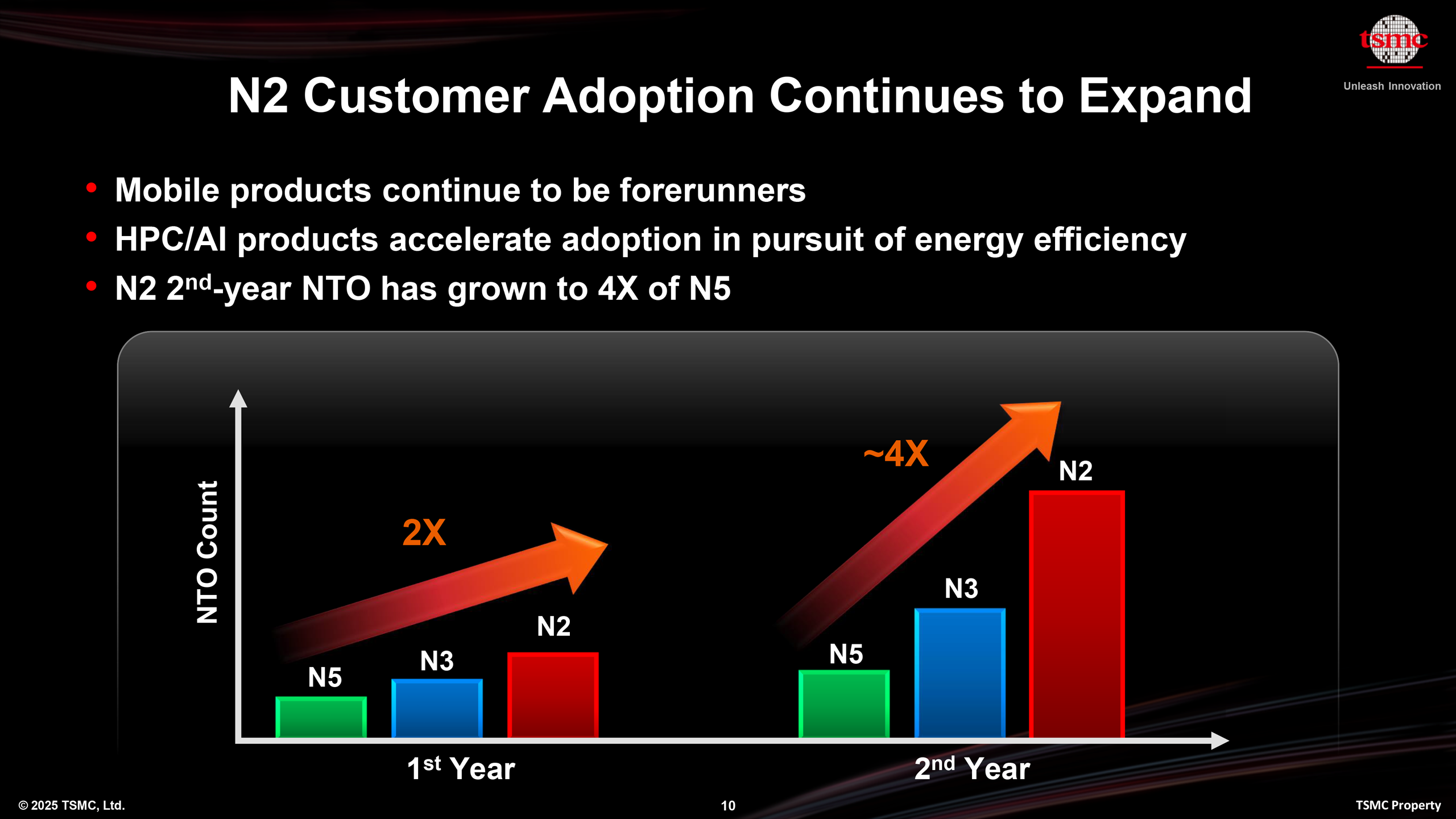
TSMC states that its N2 process node is experiencing significantly faster customer adoption than its predecessors, with the number of new tape-outs (NTOs) in its first year already doubling that of N5 at the same stage. This momentum continues to build, as second-year NTOs for N2 have reached approximately four times the count seen for N5, signaling strong market interest and early design activity.
While mobile products remain the leading adopters of N2, TSMC claims that HPC and AI customers are accelerating their use of the node, driven by the need for greater energy efficiency. This early engagement from traditionally later-stage segments (see AMD Venice example) highlights N2’s appeal across a wider range of applications compared to previous generations.
N2P and A16: Due in 2H 2026
Unlike Intel’s 18A (1.8nm-class), TSMC’s N2 does not support a backside power delivery network; however, TSMC says the new node still delivers tangible benefits even without it. In case of TSMC’s nodes, BSPDN — called Super Power Rail (SPR) — arrives with the A16 fabrication process. The foundry employs the most complex and expensive, yet most efficient, approach to backside power delivery, which involves directly connecting a backside power network to each transistor’s source and drain. This contrasts with Intel’s 18A approach, which connects BSPDN to the cell or transistor contact, a cheaper but presumably less efficient method.

Since TSMC’s SPR backside power delivery technology is expensive to manufacture, TSMC will continue to offer nodes without SPR going forward. One such process technology is N2P, which is a performance-enhanced version of N2 with a traditional power delivery network, that promises to offer 5% to 10% higher performance, and 5% to 10% lower power compared to N2.
In fact, to a large degree, A16 is N2P with backside power delivery, according to TSMC, which will enable chip designers to reuse IPs for different products. For client applications that do not need a dense power network, N2P could be an optimal solution, particularly from a cost perspective. For those who require dense backside power delivery, TSMC will offer the A16.
Both N2P and A16 are set to achieve high volume manufacturing milestone in the second half of the year, so expect actual products to hit the market in 2027.
In addition to N2, N2P, and A16, TCMC will also offer N2X, the ultimate version of N2, with enhanced voltage tolerance to enable maximum clock speeds, albeit at the cost of increased power consumption. This node will be particularly useful for high-end client CPUs and some data center offerings that require maximum single-thread performance guarantees. N2X is expected to get to mass production in 2027.


